hello
This week, I wanted to get into the weeds of working with an FPGA, following last week’s push for hardware consolidation. I had a second-hand Tang Nano 20K laying around, which is a development board built around a Gowin FPGA with about 20K look-up tables that define the internal circuit. From some initial napkin calculations, packing a Linux-capable processor, a bunch of USB buses, and a few other hardware blocks would require us to go for a 20-25K FPGA on the final product. It’s unlikely we’ll end up going with Gowin FPGAs after I saw the costs on LCSC, compared for instance to Lattice ones. That said, it’s the right caliber, so we’ll use it to experiment until I sleep on the whole FPGA approach enough to warrant a board closer to what we’ll put in the final product.
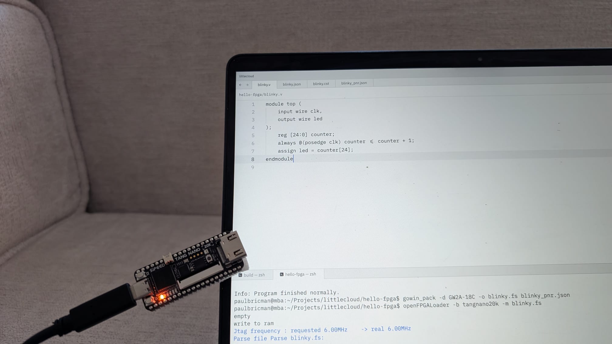
So, onto getting the FPGA to blink an LED. We need two input files, a Verilog one defining the logical behavior of the circuit, and one for generally mapping variables to specific pins on the physical chip. The Verilog in the picture below does the following. We’re defining a tiny block of circuitry that has one input and one output “wire.” We’re then effectively defining an integer over 24 bits. Then, on every rising edge of the clock signal that we tapped into, we increment that integer. Finally, we take the most significant bit of the integer and wire it to output. Basically, we’re implementing a clock divider to slow down the native 27kMhz clock by 2^24 or so, and use the resulting ~2Hz tempo to flip the LED state.
The tooling we need to “synthesize” this circuit on the FPGA is quite involved. First, I used “Yosys” to turn the Verilog into what I understand to be abstract representations of how look-up tables (LUTs) and registers need to be wired to implement the specified behavior. Then, I used “Nextpnr” (place-and-route) to assign specific blocks on this specific Gowin FPGA to those roles. Then, I used “gowin_pack” to build the previously generated JSONs into a binary the FPGA understands. Finally, I used “openFPGALoader” to flash that binary over USB to the actual board. Granted, the reason we’re dealing with four different tools here is that they’re the open source, reverse engineered alternative to Gowin’s integrated yet proprietary tooling. It boils down to four legible commands that can be scripted, could have been worse.
litex
Next day after the Verilog blink test, I decided to actually give LiteX a go. This is a library of open source cores that allows you to turn an FPGA into a System-on-Chip with exactly your specs. It has a tutorial with a few labs, so I mostly went through that first. “Mostly” because the tutorial was based on a different development board which had more outputs and sensors. I did a binary clock with the 6 LEDs on the Tang Nano 20K instead of displaying the time as digits. I also got to implement pulse width modulation, the kind of peripheral a microcontroller would use to dim an LED with a square wave, here shown as a simulated waveform.
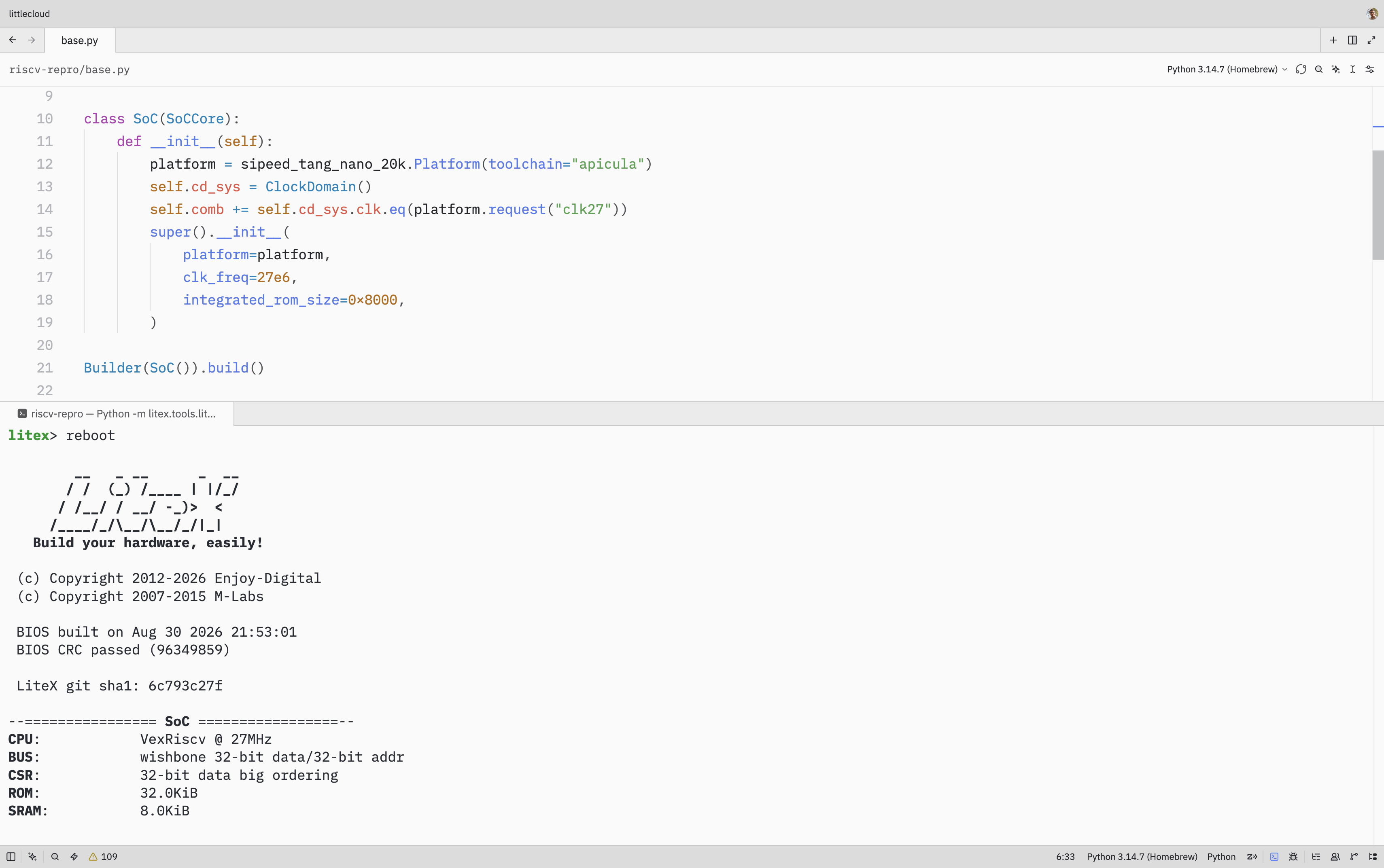
Getting a Linux-capable processor baked into the Gowin FPGA on the Tang Nano was trickier, because Linux doesn’t really fit into the 8MB of integrated RAM on the chip. So I might need to already switch to a development board that’s closer to the intended use case rather than what I had laying around. I did manage to flash a dummy shell on one of these soft cores, without loading any actual OS underneath. Apparently, LiteX also automatically builds a BIOS for your SoC definition, equipped with a debugging shell over serial. And it only takes a couple dozen lines of LiteX to define, build, and flash a SoC that exposes such a shell. Pretty neat.
While I was binging anything I could find about FPGAs on YouTube, I realized that Phil’s Lab has a course focused on designing a board that happens to incorporate an FPGA, high-speed USB, memory routing, external flash, etc. Phil’s previous course was the one I followed to learn how to use KiCAD in the first place. So I thought maybe I could take this other one too, but instead of reproducing the demo board he builds throughout the materials, I could just use the course outline as a guiding structure and apply the same principles to little cloud directly. I contacted Phil to ask whether it’d be fine to submit this other board at the end of the course for the certificate and all, and he seemed fine with it as long as it’s of a “similar complexity.” It’d be really cool to get an actual expert review on the little cloud hardware before submitting that first version to manufacturing.
bye
I had a first scare when I realized that, wait, the mere fact that there are open source USB soft cores out there doesn’t mean Linux would automatically be able to drive them with native drivers. In fact, I could only find a pair of host and device cores with native Linux compatibility, but they were only for USB full-speed (12 Mbps), not high-speed (480 Mbps). I’d really like to match the widespread high-speed found on would-be worker devices, to avoid little cloud itself being the bottleneck.
I did find the LUNA project, which brings open source USB high-speed device cores that can be controlled through software. Even if not the native Linux interfaces outright, it can do networking, mass storage, keyboard input, etc. For USB high-speed host cores, I did find guh, which again enables some use cases but falls short of full Linux compatibility. One option is to have little cloud usually emulate a USB high-speed device to everyone, including smartphones and tablets. And only use a Linux-compliant full-speed host for the mobile worker bring-up, such as for running ADB. It is possible to do both high-speed host and device from Linux, as exemplified by the proprietary IP cores that boast such capabilities, but the open source stuff is currently limited to either full-speed Linux-compliant or high-speed hand-rolled.
But a worse scare here was when I tried to get an actual empirical estimate of how many LUTs would be required for what we need here. I had GLM 5.3 Flash experiment with defining and synthesizing a few SoC variants that incorporate the specs we need. Well, the initial calculations were too optimistic, especially if you account for some way of moving traffic between USB buses themselves and from an SD card. For doing this efficiently, you either need a DMA controller per bus that copy data to RAM without processor involvement, or you need some routing between these in the actual gateware. Anyway, when I tried going from napkin calculations to having an LLM actually experiment with synthesizing a few configurations, it became pretty clear that the few FPGAs that are not crazy expensive wouldn’t have enough capacity to hold all of what we’d need them to. The search continues.
cnc
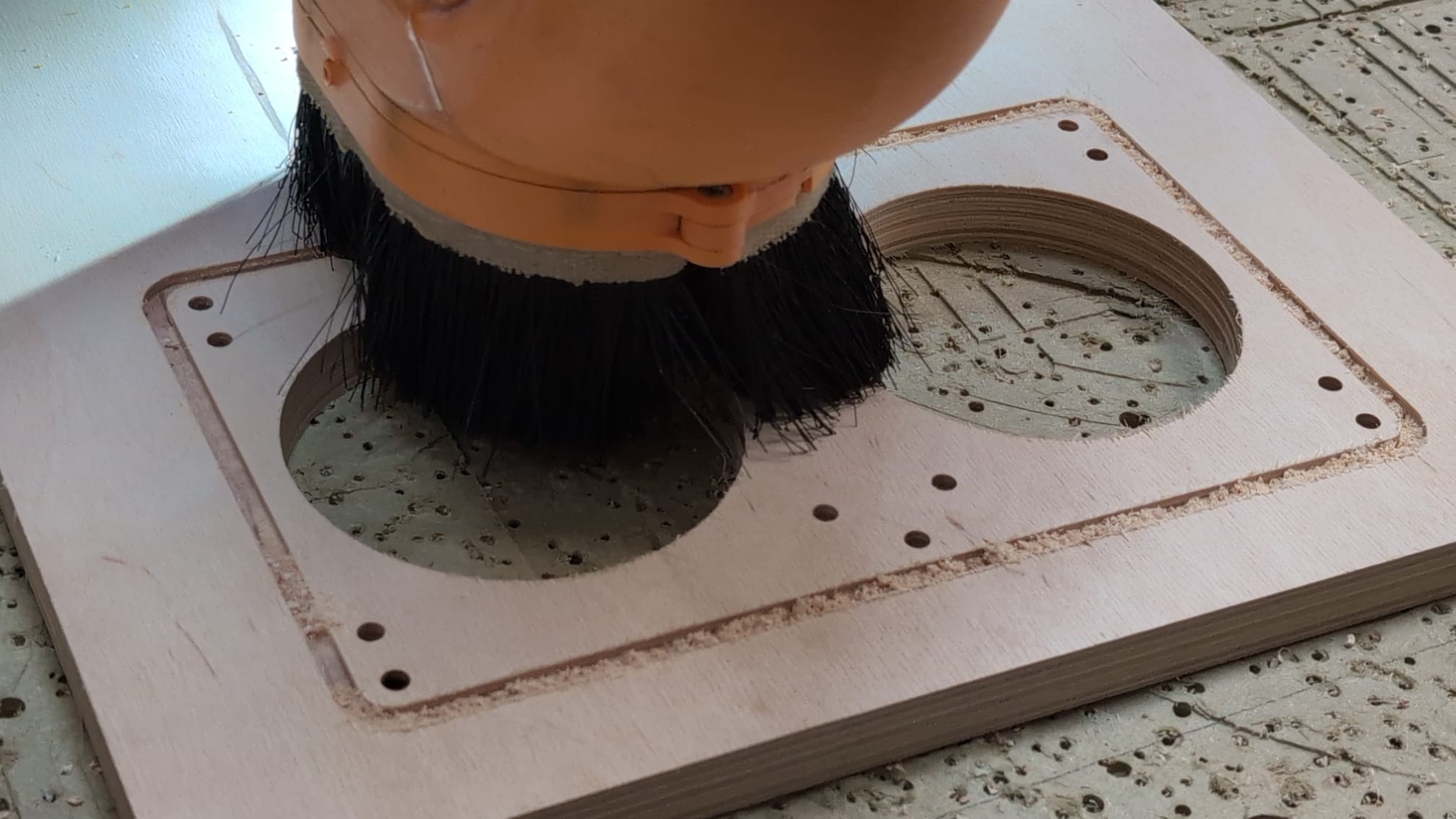
This same week, I wanted to try getting a hang of the CNC router at a local makerspace, as mentioned in entry #5. The idea was that maybe I could iterate on the enclosure faster and cheaper than working with a CNC shop. So I signed up for an intro session, during which we actually got all the way to CNC-ing a slightly tweaked file export from that same Onshape project. And we cut it out of... a glorious slab of 18mm scrap plywood that we grabbed from a discard pile. Quite a bit chunkier than the 1mm aluminum I had in mind, it feels like the volume of a whole enclosure rather than a plate.
I realized early on during the intro session to what extent the modern software of products like Bambu Lab’s A1 have spoiled me. After you export a DWG/DXF out of your CAD of choice, you first need to process it using “CAM” software, which is the equivalent of slicers in 3D printing, only way more manual and clunky (at least the AutoDesk one we worked with). Then we put it on a stick and loaded it on an ancient piece of software that controlled the actual CNC through motor drivers, which is the equivalent of Klipper in 3D printing. The CNC itself lacked vacuum suction for holding down the material, hence the countless screw marks on the working area. The spindle was powered separately, and relied on a DIY water-cooling loop. Overall it felt too janky, so I don’t think I’ll go ahead with using it for real.
fdm
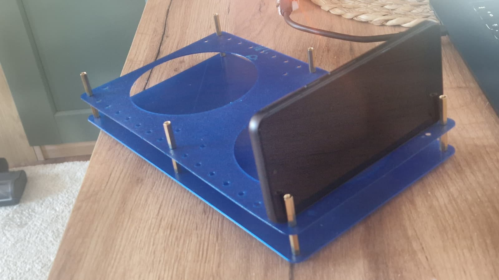
What I did try using afterwards after all was a standard 3D printer. This is mostly only relevant for the simplified flat plate “enclosure” approach described in update #5. Because of the reduced size, it fits in the build volume of an A1. Yes, it’s not actual sheet metal, but it’s enough to get a feel of the proportions.
After an initial print, I realized that the support holes for the worker devices are a bit sparse, the two rows are a bit too far from each other, and the margins make it a bit finicky to use nuts with the standoffs. A second iteration felt like a step in the right direction, though worker supports are still finicky to move around.