local
Last week left us with a consolidated collection of parts, with exact footprints and product codes on LCSC. This week, it’s all about PCB layout and routing. The key lesson I got from Phil’s Lab courses was to break down the problem into individually manageable pieces.
Actual PCB design once the schematic’s done can be split into local layout, global layout, local routing, global routing. When focusing on the local level, we work on individual islands of parts working together in a functional arrangement, roughly corresponding to the sections from the schematic. Whereas when we talk about global layout or routing, it’s a matter of further organizing these islands and handling the interaction between them in terms of relative positioning and interconnects. Splitting out the layout is another obvious way of factoring the problem into more granular ones, because layout implies a rough approximation of what would connect to what by proximity and orientation.
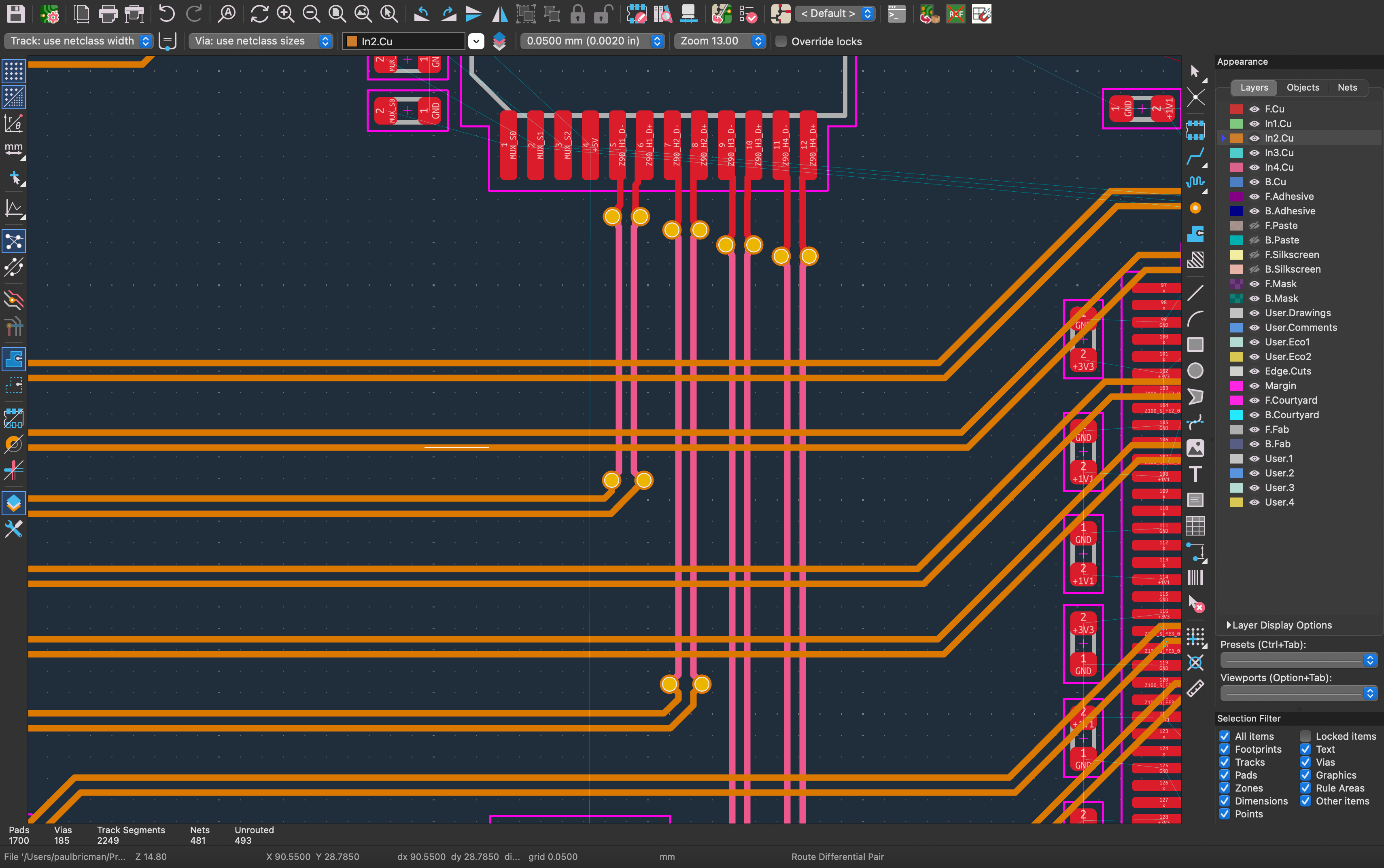
So when it comes to local layout, I went ahead and grouped together the various functional cluster in their own little islands. I tried to come up with an explicit strategy to reduce decision fatigue. Roughly, decoupling caps and strap resistors go around the chips on the same side, whereas signals get pushed through vias into internal layers. The connectors need a predictable placement also, and they’re the only ones I filled in exact coordinates for based on desired pitch. For all other components I tried to wing it by hand, which was quite uncomfortable but it would’ve taken 5x longer if I were to painstakingly place everything exactly right at this current point. Maybe after functionality is validated.
global
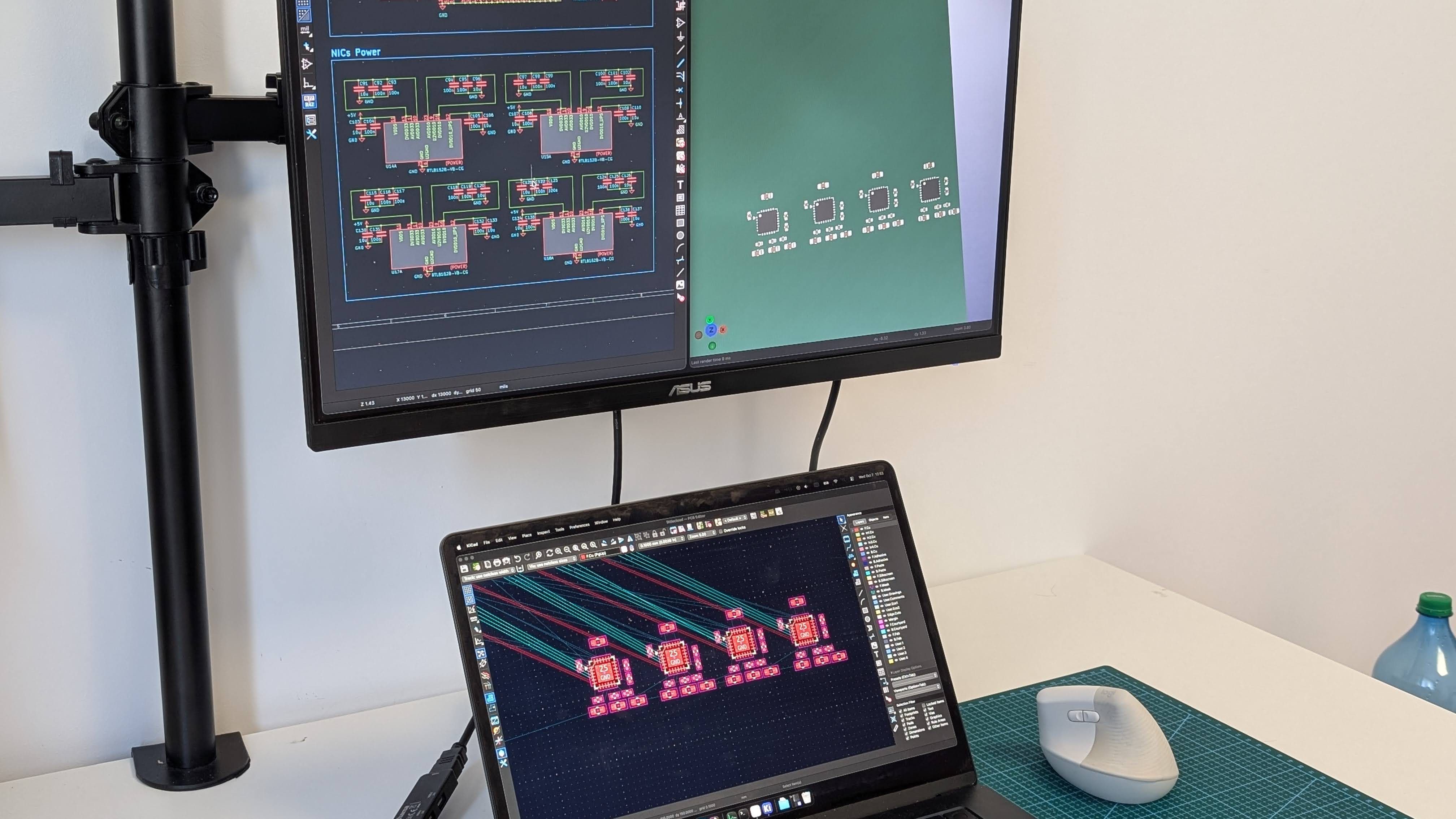
After clustering together these little islands of components, I started gradually arranging them into the right position relative to each other. Here as in all of hardware design, it’s all a matter of solving constraints. Connectors need to be on one particular edge. Power should be next to the Type-A array because the downstream worker charging will take most power. I swapped a port for USB Hosts in favor of an Ethernet port to tentatively solve the internet uplink problem and keep WiFi radios focused on increased worker-to-worker interconnect rather than connecting to a home router. This RJ45 port needs to be near the ports for USB Hosts, because each has a USB-to-Ethernet chip, and all feed into the on-board switch. This gives us networking across host workers, the System-on-Chip, and the uplink.
The corners have space for connecting to the threaded cubes in the corners, which is also the path to chassis ground for the board. I initially had one LED per port thinking it’d help indicate the intended port above it, but I dropped them for now to avoid double-sided assembly and because the sideways surface-mounted LED offering was inconclusive on LCSC. We’ll use the built-in LEDs on the RJ45 connector for now. The microSD slot on the board rather than off an edge is a bit weird, but that one is not user-focused. Moved things around quite a bit incrementally until an arrangement I was content with, generally reaching a setup where the connectors and per-port circuitry forms a row of its own, while other supporting elements sit on a separate row above it.
through-hole
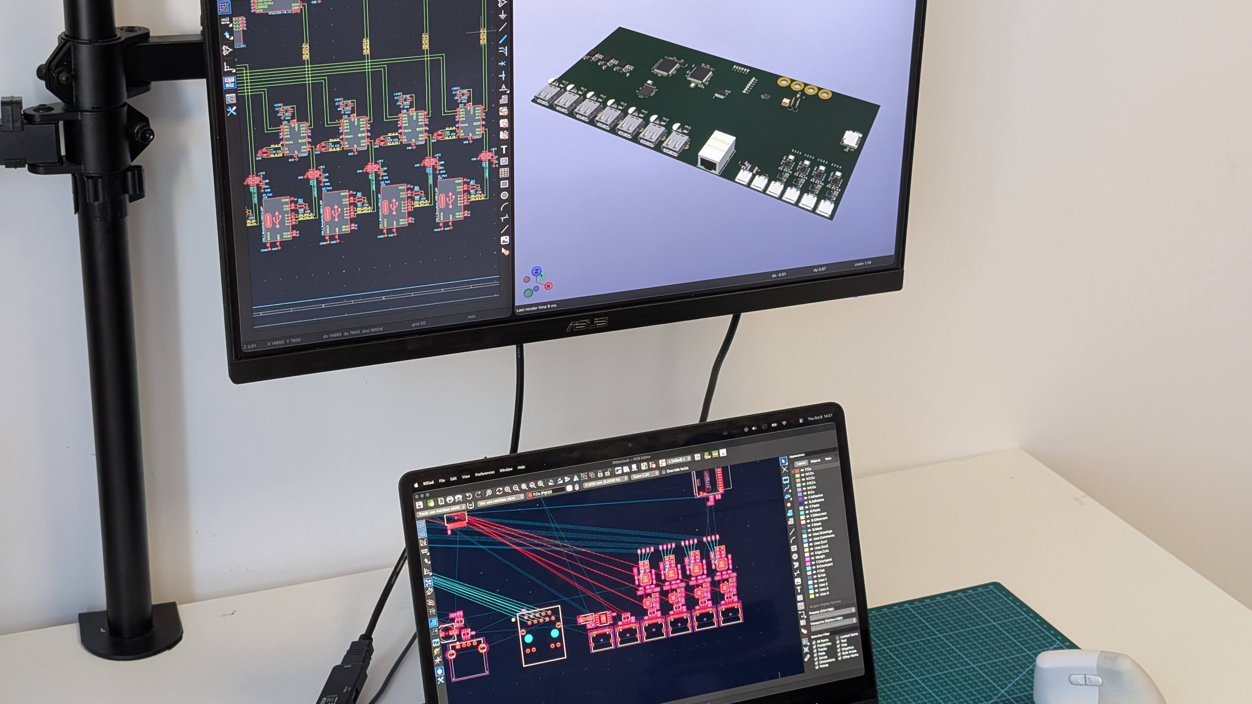
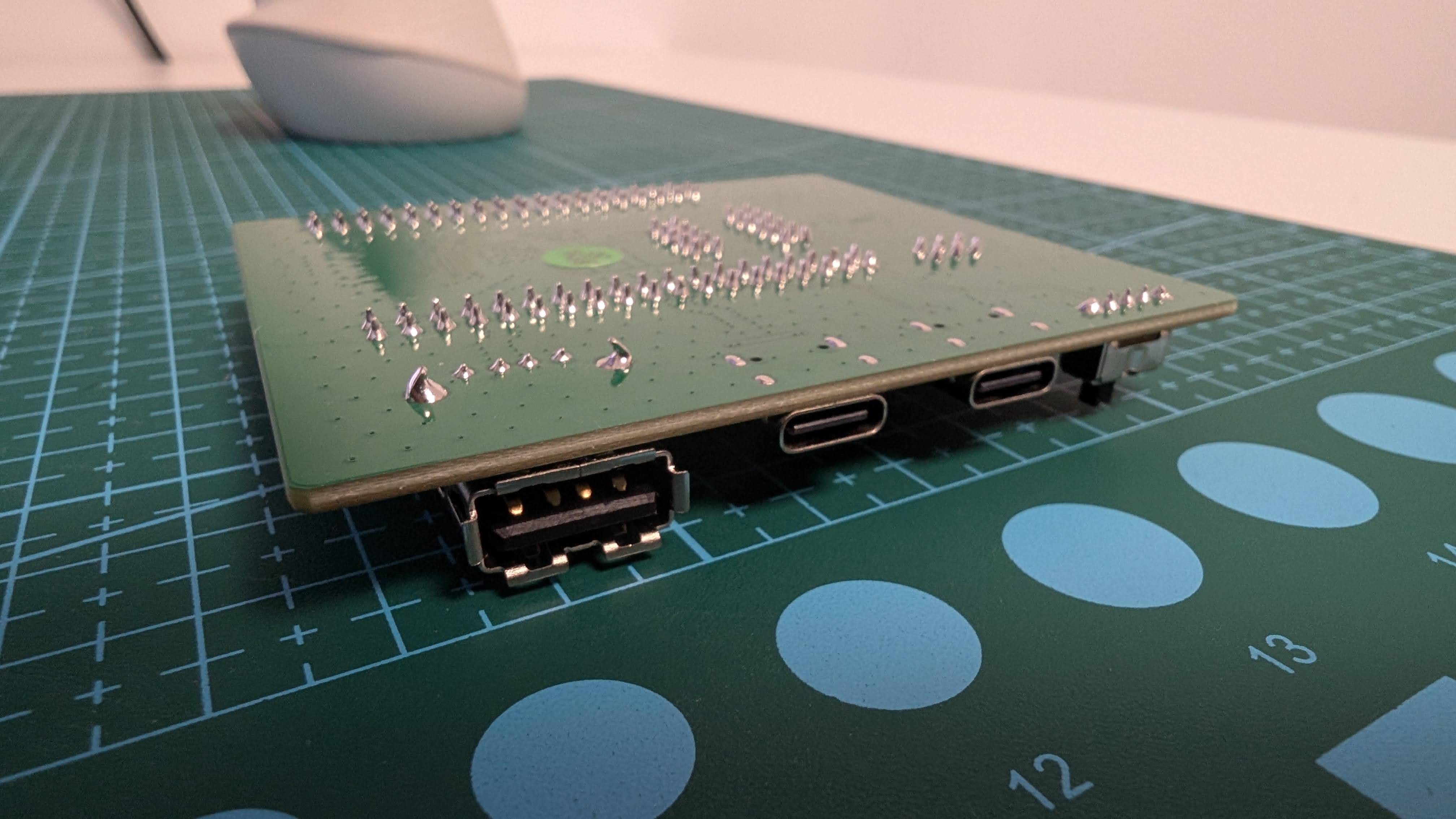
After I did a rough global layout, I was turning around the 3D model to get a feel for how things would land. And then it hit me, every single connector we’re using is through-hole. And it’s actually hard to find any variants which aren’t. This would actually make it awkward to reach for worker supports on the opposite side of the large enclosure opening. Your hand would go over solder joints, which often come out jagged. That wouldn’t be too elegant, even if we could’ve had LEDs by the port on the other side and communicate through the silkscreen.
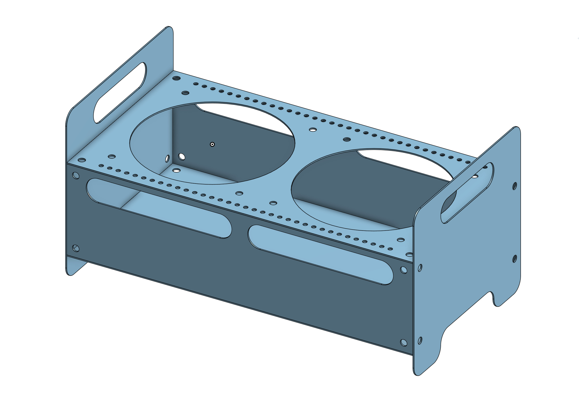
So I did another enclosure iteration. Basically, the idea was the following. Instead of a large air intake opening on the back side that was also used for configuring worker supports on both lines, let’s have smaller, subtle openings on both sides, near the top. This allows intake for the fans as before, and also allows users to reach directly to the standoff supports on either side, not having to reach through. In this setup, the PCB is more thoroughly enclosed. It’s not really visible anymore from the outside and you’re not supposed to actually touch it during normal use. Of course, we still have port cut-outs to reach the connectors, but the main interface that needs visual cues becomes the back wall as a whole. This means we’re back to laser engraving or silkscreen on that particular aluminum plate. Structure integrity is better because the back long side isn’t completely empty anymore, instead giving us support at the ends and in the middle, as the two gaps follow the fan layout. I’ll wait for the first enclosure variant to arrive so that I can use it to enform a second run. Also, RJ45 didn’t fit with 10^3 M3 threaded cubes so we do 15^3 M5 instead now.
routing
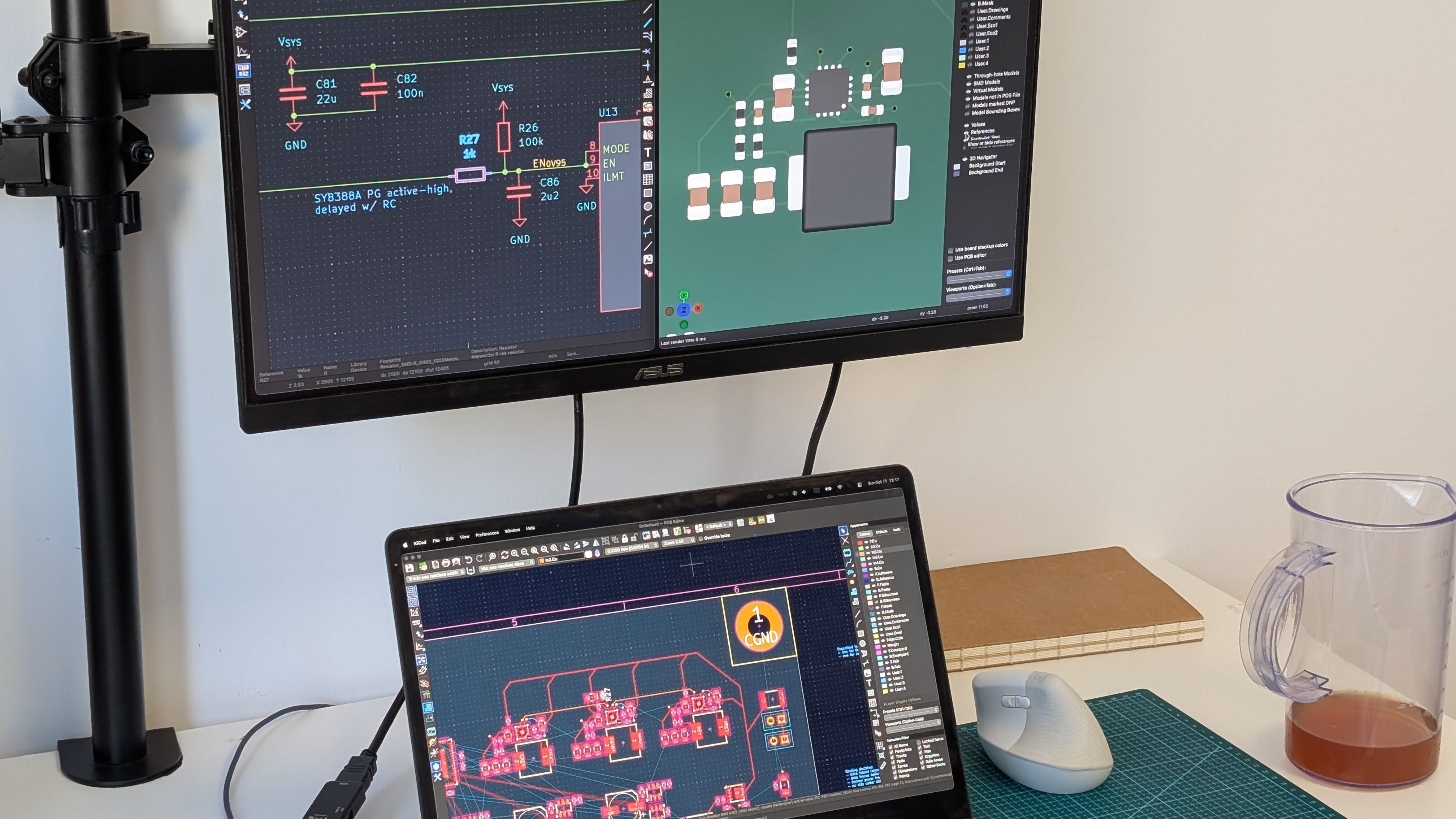
After this enclosure revision, I started going back to the local level and doing little islands of connectivity, starting with the power input cluster, then the bucks, the Type-A ports and their switches, and so on. Of course, parts moved around quite a bit once actually trying to connect things and running into issues, but the first pass in the form of separate layout proved extremely helpful. With most things being mostly in place, most connections were then trivial to establish.
I also chose to follow another simplification. No copper pours just yet, which are these whole polygons instead of trace lines that you do for power especially. Those will come later, once we’ve sketched things out with simple traces as stand-in lines. This also helped make initial routing a whole lot more approachable.
I watched a video from Phil on cost-adders over lunch and realized that there’s a minimum via size selector in the quoting system. Had to go back and make sure we’re on the cheapest, most lax tier. So I removed a few vias I got to placing and placed new ones with slightly larger diameter.
layers
As with layout, I then moved on from local to global for routing. This boils down to connecting the local stubs across distinct islands. Things got quite involved when dealing with the final boss we’ve seen earlier during the schematic. Gasp, the “Connections to USB Hosts & Uplink.” It’s the one with a while hub and NIC per port, plus the Ethernet and analog switch.
I got to a point where I seriously considering going for 8 layers instead of 6, to make it easier to connect things without collisions while trying to respect EMC and signal integrity best practices. I ended up staying on 6-layers (for now), by locally “borrowing” the L5 PWR plane for some emergency signals going into the CH448U analog switch. It’s fine, it’s probably overkill to force all signals on internal layers anyway. We’ll see during EMC testing at least. 6-layers also happens to give us “economic assembly” at JLCPCB, which is a bit cheaper but is only available for <50 volumes. So we still get standard in an actual production run, but still handy for prototyping.