
logistics
I digged deeper into approaches to logistics and fulfillment following last week’s entry. First, I realized that PCBWay runs sponsorships for non-profit and open source projects, so I took some time to apply. It’d be awesome if I could get the prototyping costs partly covered until I reach a version worth applying to Crowdsupply with. From that point on, I could potentially rely on the same manufacturing pipeline to fulfill runs through Crowdsupply’s Mouser parent. Though TME and Olimex in particular also seem like relevant and inexpensive distributors, especially in an EU context.
Also interesting is that companies like PCBWay and Elecrow can integrate manufacturing together with kitting, packaging, and direct to consumer shipping. But if you sell through their storefronts, it’s still your product and you retain the EU compliance hurdles. Maybe PCBWay or Elecrow for direct shipping outside the EU, combined with TME or Olimex to handle EU hurdles, even if they of course add their own further margin. We’ll see how the PCBWay prototyping experience goes, I hope it’d work out to scale through them without other dependencies.
order
So I did a final pass on the enclosure model before before sending it off to PCBWay. Switched to 10x10x10mm threaded cubes from 10x10x6mm pancakes. Moved the PCB to the top side of its dedicated pocket, getting us silkscreen markings around the ports. That top layer will mostly be GND with some information LEDs at most, nothing high-speed. No need to extend the PCB all the way to the other side, as well. If some power bricks are placed in the storage drawer, they can be behind the PCB, which feels better for thermals, too. Plus minor hole size adjustments and cut-out experiments for the actual Type A and C ports.
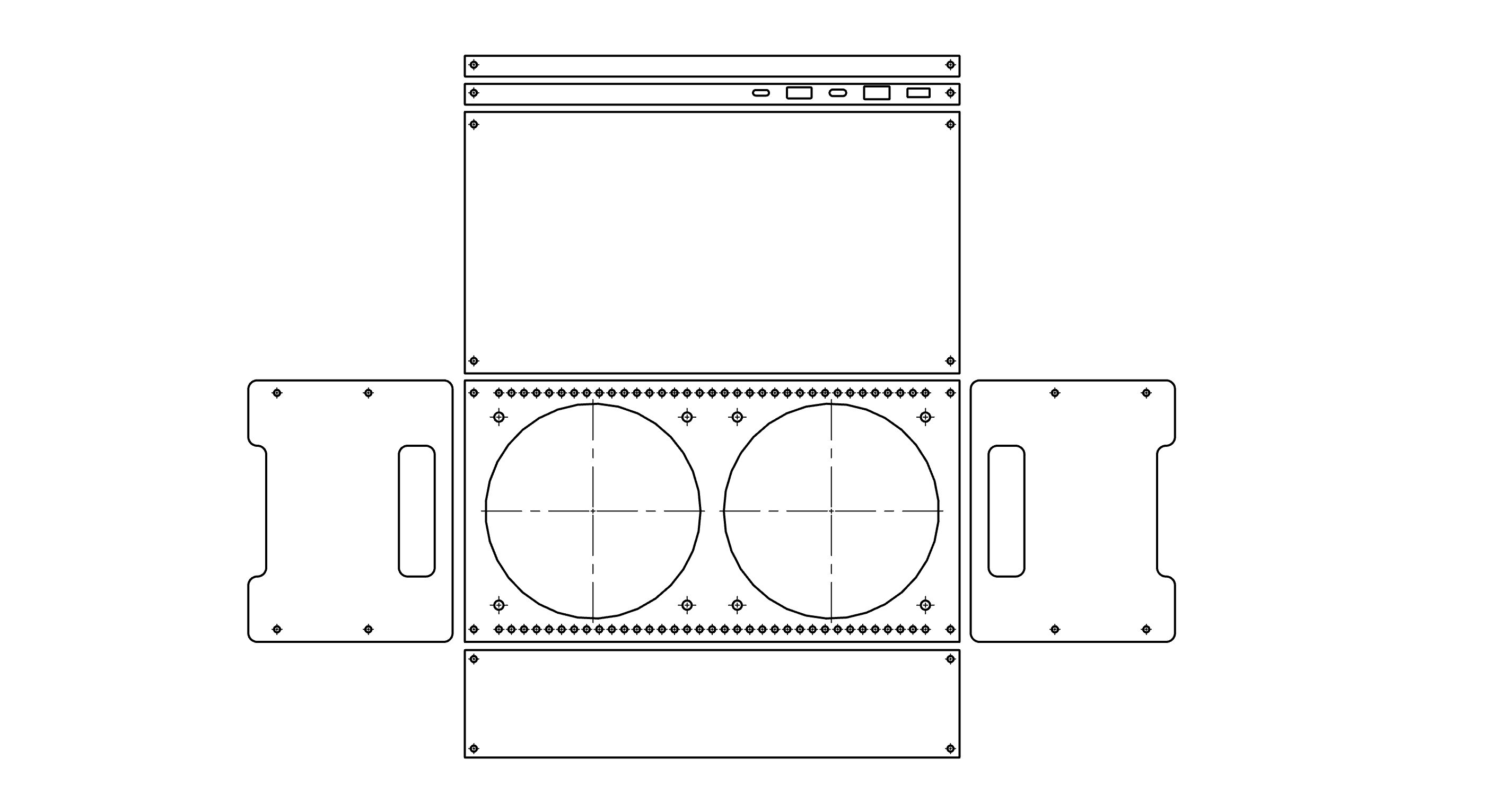
I started adding in the plates as different parts. The total price wasn’t looking great at one piece volume. However, they shouldn’t be treated as different parts, there are no bends and so it’s just a big flat piece, even if non-contiguous. Moved everything to a shared 2mm Aluminum thickness to allow same-sheet manufacturing, and arranged the different plates into a 2D drawing in Onshape. First time I did this, feels really powerful for communicating assembly instructions and what’s inside, like those Ikea manuals. So I sent the DWG output of the drawing instead. The automated quote didn’t work right away on my file, maybe I haven’t followed some conventions initially.
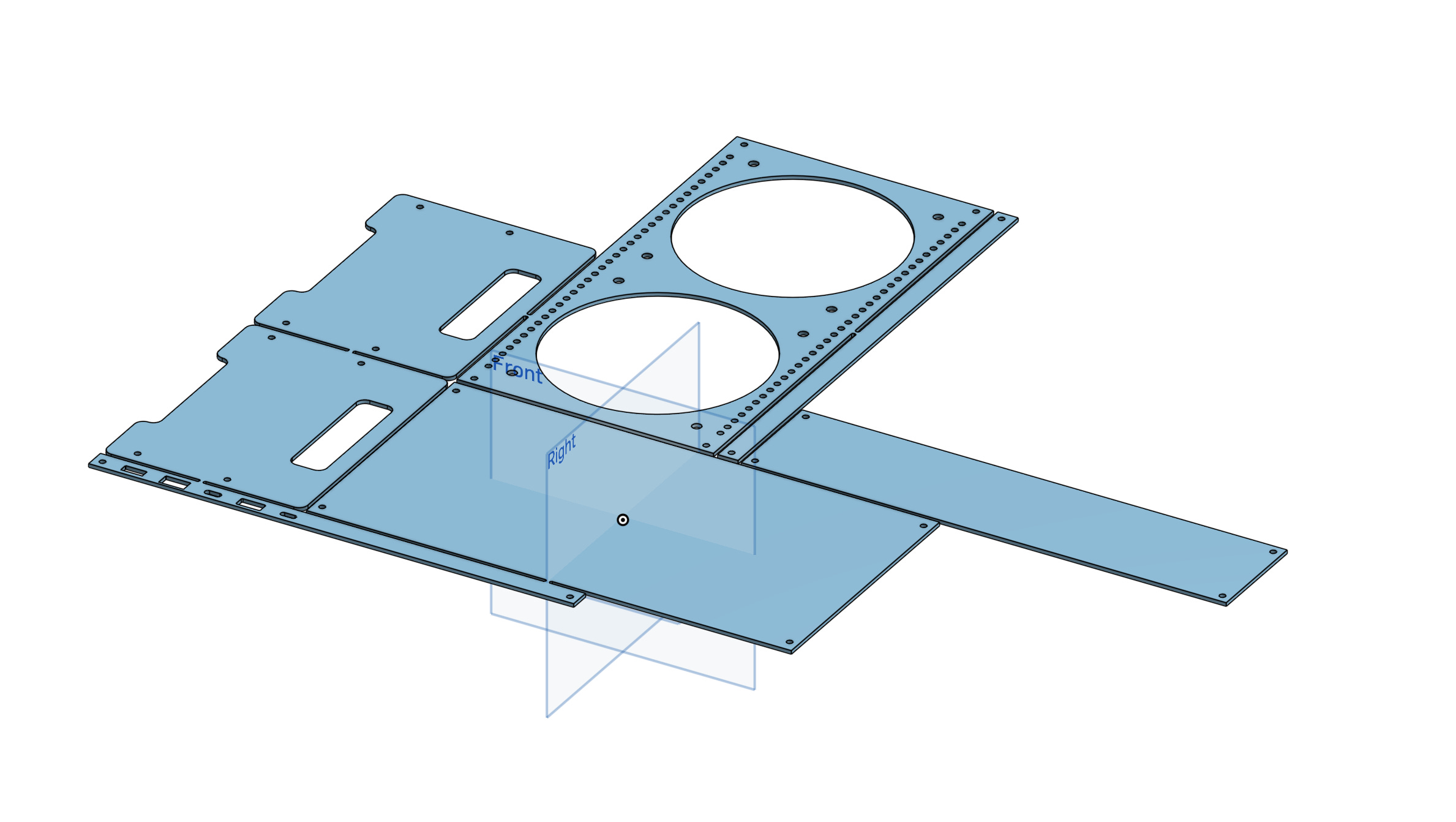
Someone responded and flagged that they’re separate parts and so should be sent separately. I was thinking, fair, they’re not a contiguous piece, so I edited it to get an actual single piece with thin tabs between plates, and I’d snap them apart at home. But nope, this didn’t go through either, and the price per part was 3-4x compared to JLCCNC. So even if I managed to get an initial PCBWay sponsorship in credits, the JLCCNC version was still cheaper after applying the credits. They seem to add a significant premium for the fact that everything’s under one roof, and they need to cover the aggressive sponsorships somehow. So if I want the rock-bottom pricing of JLCCNC and JLCPCB, I have yet to find a vendor to solve kitting, packaging, labeling, etc.

stackup
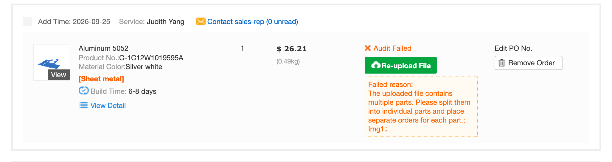
In the section above, I mentioned that the PCB moved to the top of its pocket, being partly exposed. This implicitly impacts stackup, because that exposed layer can’t be a full signal one anymore. Beyond that, during the lesson on stackup and buildup from Phil’s Lab, I realized I was too naive when thinking of going for SIG/GND/PWR/SIG in one of the first build logs. For good EMC performance, we need every SIG and PWR layers to be near a GND one. High-speed signals should ideally be flanked by two contiguous planes even, so routed on internal layers.
If we go to a 6-layer PCB, we could follow these guidelines by doing SIG/GND/SIG/GND/PWR/GND, with a handful of low-speed signals on the exposed outer GND layer to populate the silkscreen. Going to 8-layers on a similar pattern would buy us another internal SIG, not sure if it’d be worth it. We’ll see during routing.
pdn
The power distribution network feels like the most intimidating part of the system, to be frank. For routing data signals it’s mostly making sure to use controlled impedance, spacing out traces, and keeping them short. For power, we need to derive 4 power rails just for the on-board components. In contrast to the ZettBrett board discussed in the Phil’s Lab course, we also want to charge downstream USB devices, which make up the bulk of the load.
To keep it manageable for this version, I looked for various corners to cut. At some point I thought it’d be cool for laptops to provide emergency power to little cloud’s on-board systems, but merging that with the standard upstream power seemed tricky. So, gone. Maybe a battery slot to effectively add an internal UPS for little cloud’s essential systems? Detecting it and caring for it adds further complexity, gone. Most USB-C chargers have ports that go up to 15/20/25W, maybe we could have two power input ports to access more power with standard parts? Hard to merge the sources, gone. Maybe we could vary the configuration pins on downstream Type-C ports to advertise 5V@0.5/1.5/3A to charged devices, depending on the power budget. Type-C ports aren’t allowed to be “hot” with power by default, we’d need voltage sensing to detect a sink via an ADC or comparator. So, gone. “Hardware is only as hard as you make it.”
Here’s what we’re left with. One upstream port that needs around 25-30W PD. No backfeed from laptops. Downstream smartphones and tablets only get a standard 5V@0.5A via Type-A ports, totaling 15W peak. Bonus: lowest possible wear on the worker device batteries. We have power rails for internal housekeeping, plus a separate one for ports, even if also 5V. Just like in the course, an identical wide-input buck converter arrangement per rail, stepping down from some default contract at 9/12/15V negotiated by the upstream PD controller. I picked a Silergy buck, like in the course, but rated for 5A output to cover 6*0.5A ports comfortably. Also picked an WCH power switch to use per charging port, plus we need a different hub variant hub with per-port power enable pins after all. We’ll do TVS diodes and fuses later, as refinements.